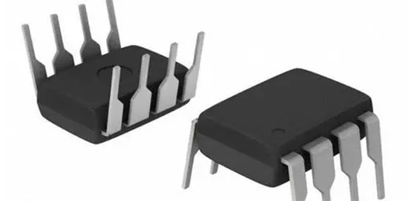
what does a semiconductor do
Introduction
Matter exists in a variety of forms; solids, liquids, gases, plasma, etc. We usually call materials with poor electrical conductivity, such as coal, artificial crystals, amber, ceramics, etc., insulators. And the metals with better conductivity such as gold, silver, copper, iron, tin, aluminum, etc. are called conductors. The material between conductor and insulator can be simply called semiconductor. Compared with conductors and insulators, the discovery of semiconductor materials is the most recent, until the 1930s, when the material purification technology improved, the existence of semiconductors is really recognized by the academic community
A semiconductor is a material whose electrical conductivity is between that of a conductor and an insulator at room temperature. A semiconductor is a material with controllable electrical conductivity ranging from insulator to conductor. From the point of view of scientific, technological and economic development, semiconductors influence people's daily work life, and it was not until the 1930s that this material was recognized by the academic community.
The discovery of semiconductors can actually be traced back to a long time ago.
In 1833, British scientist Faraday, the father of electronics, was the first to discover that the resistance of silver sulfide changed with temperature differently from that of ordinary metals, which generally increases with temperature, but Faraday found that the resistance of silver sulfide material decreased with the rise of temperature. This was the first discovery of the semiconductor phenomenon.
Soon after, in 1839, Becquerel in France discovered that the junction formed by contact between a semiconductor and an electrolyte produces a voltage when exposed to light, which is later known as the photovoltaic effect, and this was the second property of the discovered semiconductor.
In 1873, Smith in England discovered the photoconductivity effect of selenium crystalline materials with increased electrical conductivity under light, which is the third property of semiconductors.
In 1874, Braun in Germany observed that the conductivity of certain sulfides is related to the direction of the added electric field, i.e., its conductivity has directionality, and it is conductive when a positive voltage is added at both ends of it; if the voltage polarity is reversed, it is not conductive, which is the rectification effect of semiconductors, and the fourth property unique to semiconductors. In the same year, Schuster also discovered the rectification effect of copper and copper oxide.
From 1879 to 1947 was the foundation stage, the revolution in physics at the beginning of the 20th century (relativity and quantum mechanics) led to the understanding of the nature of the microscopic world (atoms and molecules), then these new theories were successfully applied to new fields (including semiconductors), the solid energy band theory laid a solid theoretical foundation for semiconductor technology, and advances in material growth technology laid the material basis (semiconductor materials require very pure matrix materials with very precise doping levels).
Although these four properties of semiconductors were discovered successively before 1880, the term semiconductor was not first used by Kauneberger and Wise until about 1911. And the summary of these four properties of semiconductors was not completed until December 1947 by Bell Laboratories.
In October 2019, an international team of researchers claimed that the new technique could obtain up to seven parameters per test light intensity compared to only three parameters obtained in conventional Hall measurements: including electron and hole mobilities; loadon density in light, recombination lifetimes, and diffusion lengths of electrons, holes, and bipolar types.
In 2022, researchers discovered that cubic boron arsenide is one of the best semiconductors known to science and is known as a champion semiconductor.
Classification and Properties
(1) Elemental semiconductors. Elemental semiconductors are semiconductors composed of a single element, of which silicon and selenium have been studied earlier. It is a solid material with semiconductor properties composed of the same elements and is susceptible to changes due to trace impurities and external conditions. At present, only silicon and germanium have good performance and are widely used, and selenium is used in the field of electronic lighting and optoelectronics. Silicon is used more in the semiconductor industry, which is mainly influenced by silicon dioxide, which can form a mask on the device production, which can improve the stability of semiconductor devices and facilitate automated industrial production.
(2) Inorganic synthetics semiconductors. Inorganic synthetics are mainly through a single element to form semiconductor materials, of course, there are also multiple elements to form semiconductor materials, the main semiconductor properties are group I and V, VI, VII; group II and IV, V, VI, VII; group III and V, VI; group IV and IV, VI; V and VI; VI and VI combined compounds, but by the properties of the elements and However, not all compounds can meet the requirements of semiconductor materials due to the properties of the elements and the way they are made. This semiconductor is mainly used in high-speed devices, and transistors made of InP have higher speed than any other materials, and are mainly used in optoelectronic integrated circuits and nuclear radiation resistant devices. For materials with high conductivity, they are mainly used in LEDs, etc.
(3) Organic compound semiconductors. Organic compounds are compounds containing molecules containing carbon bonds, and organic compounds and carbon bonds vertically, superimposed in such a way that they can form a conduction band, and through chemical additions, they can be allowed to enter the energy band so that conductivity can occur, thus forming an organic compound semiconductor. This semiconductor is characterized by low cost, good solubility, and easy processing of light materials compared to previous semiconductors. The conductivity can be controlled by controlling the molecules, and the applications are relatively wide, mainly for organic films and organic lighting.
(4) Amorphous semiconductors. It is also called amorphous semiconductor or glass semiconductor and belongs to the class of semiconducting materials. Amorphous semiconductors, like other amorphous materials, are short-range ordered and long-range disordered structures. It is formed mainly by changing the relative positions of the atoms and changing the original periodic arrangement to form amorphous silicon. The main difference between the crystalline and amorphous states is whether the atoms are arranged with a long program or not. It is difficult to control the properties of amorphous semiconductors, and with the invention of technology, amorphous semiconductors came into use. This fabrication process is simple and is mainly used in engineering classes and has good results in light absorption and is mainly used in solar cells and liquid crystal displays.
(5) Intrinsic semiconductor: the semiconductor that contains no impurities and has no lattice defects is called intrinsic semiconductor. At very low temperatures, the valence band of the semiconductor is full band, subject to thermal excitation, some of the electrons in the valence band will cross the forbidden band into the higher energy vacant band, the presence of electrons in the vacant band becomes the conduction band, the valence band is missing an electron after the formation of a positively charged vacancy, called a hole. The hole conducting is not the actual movement, but an equivalent. The electrons conduct electricity when the electrons are equipotent holes move in their opposite direction. [5] Their directional motion in the presence of an external electric field results in the formation of macroscopic currents called electron-conducting and hole-conducting, respectively. This mixed type of conductivity due to the creation of electron-hole pairs is called intrinsic conductivity. The electrons in the conduction band fall into the holes and the electron-hole pairs disappear, which is called compounding. The energy released during compounding becomes electromagnetic radiation (luminescence) or thermal vibrational energy of the lattice (heat generation). At a certain temperature, electron-hole pair generation and compounding exist simultaneously and reach dynamic equilibrium, when the semiconductor has a certain carrier density and thus a certain resistivity. When the temperature increases, more electron-hole pairs are produced, the carrier density increases, and the resistivity decreases. Pure semiconductors without lattice defects have a higher resistivity and are not much used in practice.
Application areas
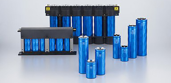
Semiconductors are used in applications such as integrated circuits, consumer electronics, communication systems, photovoltaic power generation, lighting applications, and high-power power conversion.
Photovoltaic applications
The photovoltaic effect of semiconductor materials is the basic principle of solar cell operation. At this stage, photovoltaic applications of semiconductor materials have become a major hit, and is currently the fastest growing and best developed clean energy market in the world. Solar cells are mainly made of semiconductor materials, the main criterion for judging the merits of solar cells is the photoelectric conversion rate, the higher the photoelectric conversion rate, the higher the efficiency of solar cells. Depending on the semiconductor material used, solar cells are classified as crystalline silicon solar cells, thin-film cells, and III-V compound cells.
Lighting Applications
LED is a semiconductor light-emitting diode built on a semiconductor transistor , the use of LED technology semiconductor light source is small, can achieve flat packaging, low heat generation, energy efficient, long product life, fast response time, and green, non-polluting, can also be developed into thin and short products , once introduced , it has rapidly become popular, a new generation of high-quality lighting source, has been widely used In our life. Such as traffic lights, backlighting of electronic products, city night landscape beautification light source, indoor lighting and other fields, have applications.
High-power power conversion
The conversion of AC and DC power is very important for the use of electrical appliances, is the necessary protection of electrical appliances. This requires the use of power conversion devices. The high breakdown voltage strength, wide band width, and high thermal conductivity of silicon carbide make SiC semiconductor devices very suitable for applications with high power density and switching frequency, of which power conversion devices are one. The high temperature, high voltage, and high frequency performance of SiC components has led to a wide range of applications such as deep well drilling, inverters in power generation, energy converters in electric hybrid vehicles, and traction power conversion in light rail trains. Due to SiC's own advantages and the current industry need for lightweight, high conversion efficiency semiconductor materials, SiC will replace Si as the most widely used semiconductor material.